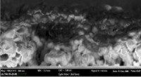
Materialforskaren Gregory Doerk i materialbearbetningslabbet vid CFN. Kredit:Brookhaven National Laboratory
Vissa material har den unika förmågan att självmontera till organiserade molekylära mönster och strukturer. Materialforskaren Gregory Doerk från Electronic Nanomaterials Group vid Center for Functional Nanomaterials (CFN)—en US Department of Energy (DOE) Office of Science User Facility vid Brookhaven National Laboratory—drar fördel av denna förmåga i material som kallas blocksampolymerer. Genom att använda dessa självmonterande material, som har kedjor av två eller flera distinkta molekyler sammanlänkade genom kemiska bindningar, Doerk styr bildandet av sådana mönster och strukturer på nanoskala. Det slutliga målet är att utnyttja dessa nanoskala arkitekturer för att kontrollera egenskaperna hos material för applikationer inklusive solenergiomvandling och lagring, katalys, och optik.
Självmontering har fått mycket uppmärksamhet nyligen som ett tillvägagångssätt för nanotillverkning. Hur skiljer det sig från det tillvägagångssätt som traditionellt har använts?
I stort sett, det finns två plattformar för nanotillverkning. En plattform är top-down nanotillverkning, vilket är det traditionella tillvägagångssättet som används för att tillverka datorchips och annan mikroelektronik. Ljus används för att skapa mönster som sedan skärs in i kiselwafers. Mönstertekniken som använder ljus kallas optisk litografi. Det andra tillvägagångssättet är bottom-up nanotillverkning, eller molekylär självmontering. Materialens egenskaper är kodade i deras svaga interaktioner, som driver vissa material att mötas och bilda specifika konfigurationer - ungefär som legoklossar men alla klossar byggs upp av sig själva för att bilda någon struktur.
Litografi är i allmänhet snabbare – och producerar mer tillförlitligt de designade strukturerna – men kräver dyra, komplexa verktyg. Självmontering är ofta långsammare och mindre förutsägande men det är billigt och kan vara lättare. Det finns sätt att kombinera de två tillvägagångssätten, och den kombinationen är känd som riktad självmontering. Självmonterande material som tunna filmer av blocksampolymerer beställs med mallar mönstrade med standardlitografi. Riktad självmontering förbättrar nuvarande tillverkningsprocesser, utöka spektrumet av mönstergeometrier som är möjliga, och sänker kostnaderna för nanotillverkning.
Din självmonteringsforskning är fokuserad på blocksampolymerer. Vad är det som gör dessa material så speciella?
Sedan 1950-talet, människor har använt triblock-sampolymerer (tre polymerer sammanfogade) i material som syntetiskt gummi. De flesta polymerer kommer inte att blandas. Att försöka blanda polymerer är ungefär som att försöka blanda olja och vatten.
Men i blocksampolymerer, polymerkedjorna är kemiskt bundna till varandra. Till exempel, diblock (två) sampolymerkedjor är sammanfogade genom en kovalent bindning. Denna bindning frustrerar deras drivkraft att "demixa". Istället, om blocksampolymerer ges energi för att mobilisera sina kedjor – till exempel genom att glödga (värma) polymerfilmen på en värmeplatta till över dess glastemperatur (när en polymer övergår från en hård, glasartat material till ett mjukt, gummiliknande) — kedjorna kommer att omkonfigureras och monteras till fasseparerade domäner i nanoskala. Dessa domäner är ordnade i nanoskala mönster baserat på inneboende egenskaper hos blocksampolymeren. Till exempel, låt oss säga att vi har två polymerer, A och B, sammanfogade (disegmentsampolymer). Längden på block A i förhållande till längden på båda blocken, polymerkedjornas totala längd, och polymerernas egenskaper och styrkan i deras interaktion (hur mycket polymererna vill dra isär) styr storleken och morfologin, eller form, av de resulterande strukturerna. Om kedjorna är för korta eller deras frånstötande interaktioner är för svaga, polymererna kommer att blandas, vilket gör att det ordnade tillståndet blir ett oordnat tillstånd och därmed kommer inget mönster att bildas.
På CFN, en stor del av vårt arbete är att överföra mönster och strukturer som skapats genom självmontering, elektronstrålelitografi, eller optisk litografi vid vår nanofabrikation i andra material för att kontrollera materialegenskaper. Ett bra exempel på detta är CFN-direktör Chuck Blacks arbete med blocksampolymerer för att skapa ett självmonterat mönster som fungerar som en mall för att etsa koner i nanostorlek på silikonytor. Med dessa nanotexturer, kiselytorna förvandlades från reflekterande speglar till helt svarta. Det är ett sätt vi kan använda blocksampolymerer på.
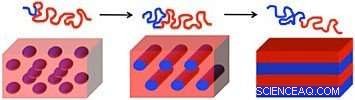
Längden på polymerblocken (röda och blå snirkliga linjer) och styrkan i deras interaktion bestämmer formen på de resulterande mönstren vid självmontering av blocksampolymer:(från vänster till höger) sfärer, cylindrar, och lameller (lakan). Kredit:Gregory Doerk
But we want to expand the range of things we can do with self-assembly—and thus the range of applications. Diversifying the patterns possible with block copolymer self-assembly is a big part of my research.
Have you been able to expand this range?
One way I am interested in expanding what we can do through self-assembly is by creating inorganic replicas of the self-assembled structures. We can accomplish this replication through a process called infiltration synthesis.
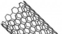
Till exempel, say you have a block copolymer that forms lamellae (stripes) perpendicular to a substrate. Using an atomic-layer-deposition tool, it is possible to infiltrate those lamellae with a metal oxide and then remove the polymer, leaving behind metal oxide lines in a pattern determined by the polymer self-assembly. It is even possible to perform self-assembly and replica formation on top of previous replicas in an iterative way. What is really interesting is that the topography from the initial layer actually acts as a template dictating how polymer domains in the next layer line up. In the case of a second layer of lamellae perpendicular with the substrate, a self-assembled nanomesh is naturally created.
What other ways can you expand the range of self-assembled patterns?
One area in which I have collaborated with other members of the Electronic Nanomaterials Group is to study the blending of block copolymers that form lamellae with block copolymers that form cylinders. The really cool thing we learned is that you can precisely control which of these two patterns emerge in different areas of a substrate through an approach we call selective directed self-assembly. In a diblock copolymer, one of the blocks may be relatively more hydrophobic (water repelling) and the other may be relatively more hydrophilic (water attracting). So if a chemical pattern was made up of alternating hydrophobic and hydrophilic lines, the block copolymer molecules would self-assemble accordingly. By changing the spacing and width of the chemical line gratings (patterns) on the substrate, we were able to direct the self-assembling blocks into specific arrangements—either forming striped patterns (lamellae) or hexagonal dot arrays (cylinders). We can locally adjust the spacing and linewidth of the underlying chemical template to precisely control exactly where these line or dot patterns form on the same substrate, för.
How big are the features of these self-assembled nanoscale patterns?
Block copolymers typically self-assemble into ordered periodic structures with a tunable repeat spacing between around 25 to 50 nanometers. Faktiskt, one of the projects I am currently working on is to increase the size range over which block copolymers form patterns. There is a lot of work in the scientific community to go to smaller and smaller sizes (approaching a few nanometers) for lithographic applications such as making computer chips. But for certain applications, you need larger sizes.
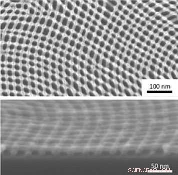
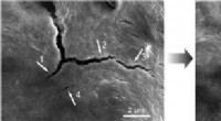
Plan view (top) and cross-sectional (bottom) scanning electron microscope images of an inorganic nanomesh created through iterative self-assembly and infiltration synthesis. Credit:Gregory Doerk
Till exempel, the wavelength range of visible light is about 400 (purple) to 700 (red) nanometers. Even 400 nanometers is still about 10 times larger than the approximately 40-nanometer length scale possible with most block copolymers. Som ett resultat, light does not "see" the individual features of block copolymers.
Dock, patterns with features closer to 200 nanometers in size can influence light in new ways, and I am working to scale block copolymer assembly to these sizes. One exciting application is using this approach to make "structural colors." Colors are typically made using dyes or pigments. Dock, structural colors emerge from the way the light interacts with the nanomaterial—and so potentially one could make new types of lower-power displays through structural color.
Tyvärr, the process of forming patterns from block copolymers slows drastically, and even stops altogether, for these larger sizes. The development of self-assembled patterns is impeded by defective structures that form at the start of self-assembly. For these defects to "heal, " the block polymer must reconfigure, which involves pulling one chain through the domain of the other polymer, overcoming a large energy barrier to do so. As the size of the polymers increases, the energy barrier goes up exponentially—so exponentially slower healing!
Have you come up with any solutions to overcome this challenge?
My colleagues and I found that blending small-molecular-weight homopolymers (polymers made up of the same type of molecules) with the block copolymers makes it easier for the block copolymer chains to move around. Adding homopolymers promotes dramatic increases in the size of well-ordered pattern areas, or "grains." Dock, this addition alone does not let us form patterns with larger-size features from block copolymers. We also need to anneal the materials in a solvent vapor. Solvent vapor annealing involves putting a volatile solvent in the region of the diblock copolymer, causing the polymer film to swell. As the polymer film swells, the solvent molecules intersperse between polymer chains. This process has a plasticizing effect, making it easier for the polymer to move. So both mixing the block copolymer with a homopolymer and swelling it with a solvent are needed to speed the formation of large-scale patterns.
After annealing, we image the resulting patterns with scanning electron microscopes at CFN. We also perform x-ray scattering experiments at the Complex Materials Scattering beamline at Brookhaven Lab's National Synchrotron Light Source II [also a DOE Office of Science User Facility] to get a measure of the periodicity during the annealing process so we can determine how quickly the material self-assembles into an ordered pattern.
How do all of the different self-assembled patterns you generate translate to possible applications?
The work we do at CFN establishes the basis for producing new materials. Till exempel, consider the mesh pattern I described. My colleague Chang-Yong Nam and I are working on making a mesh of zinc oxide nanowires through infiltration synthesis of block copolymers. Zinc oxide is a versatile semiconducting material, and these nanowires have a lot of surface area, making them attractive for a number of applications—including photoelectrochemical water splitting (a way of converting sunlight into fuel by splitting water into hydrogen and oxygen). These semiconducting nanowires are also very responsive to environmental cues like light or chemicals. Given their large area uniformity, the meshes could be easily integrated into widely deployable gas sensors.
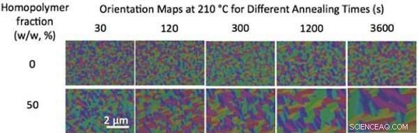
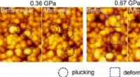
Without blending, the size of grains (single-color regions) of a diblock copolymer with a molecular weight of 36 kilograms/mole barely changes with thermal annealing over time (top row). Blending the block copolymer with homopolymers increases the grain size and speeds up the ordering process (bottom row). Credit:Gregory Doerk
How did you come to join CFN?
After graduate school, I completed a postdoctoral appointment working at IBM in California. It was there that I learned about block copolymers, using them to make patterns for microelectronics. I did that for three years, and then in 2013 I joined a research group at HGST, a subsidiary of Western Digital that sells hard disk and solid-state drives. I början, I worked on a project to create patterned nanoscale magnetic media onto which data is written to and read from, in order to enhance data density and stability.
Following that project, I moved into another area that was not very research oriented. At about this time, the current CFN Director, Chuck Black, gave a talk at HGST. Chuck's talk piqued my interest in CFN, and soon thereafter a position that very well fit my skills opened up. I applied, and joined CFN in 2015.
What was it like coming from industry to a national lab setting?
It definitely takes some getting used to. There is a lot less pressure in some ways but more pressure in other ways. At CFN, you are expected to develop a lot more on your own as far as what direction you need to pursue on the basis of what is valuable to the lab. Inom industrin, the goals of the project are clear, and there are deliverables to keep you on the narrow path to achieving those goals. This is not to say that I did not do exploratory research for a portion of my time in industry.
The other difference at CFN is that I am more involved with the academic and industrial community at large. I have to manage my time so that I can perform my own research and help users with their research. I find it really cool that researchers from all over the world come to CFN. The talent and expertise of the staff are what make the CFN so great. The staff know backwards and forwards what they are doing in the areas they specialize in, and they are dedicated to helping others.
What are some of the ways you have helped users?
I regularly show users how to do block copolymer self-assembly and the etching process to transfer patterns into a substrate. Some users have employed these patterns as superhydrophobic textures to manipulate the flow of liquids in microfluidic devices, till exempel. I många fall, I help users develop a process when they need self-assembled patterns of varying sizes or shapes, to be applied to different substrates.
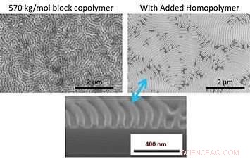
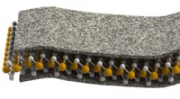
A comparison of scanning electron microscope images after solvent vapor annealing of a large block copolymer (top left) and the same copolymer with added homopolymer (top right) shows that the homopolymer can significantly improve pattern quality. The bottom image is a cross-sectional image of the top right sample. Credit:Gregory Doerk
I also help with the lithographic patterning of unusual materials. Till exempel, one user I am working with is trying to pattern protein hydrogels, looking at how they mechanically respond to swelling and de-swelling to understand how they might operate if injected into the body. Such protein hydrogels could have applications in biosensing, drogleverans, and wound healing.
Some users are interested in solvent vapor annealing, which is a very tricky process to control. So I am building a system with feedback control that can be set to maintain a solvent fraction of any given solvent. Annat, if the amount of solvent varies over time, the self-assembly might not work at all (too little solvent) or result in a disordered state (too much solvent).
How did you become interested in research?
As an undergraduate at Case Western Reserve University, I majored in chemical engineering. One of my summer internships involved doing fuel cell work at a research lab. This internship led to another one at a fuel cell start-up, where I worked on sensors and solar cells. These internships gave me the opportunity to come up with ideas of my own and try different things. This exploration spurred me to pursue a doctoral degree at the University of California, Berkeley, where I continued my studies in chemical engineering.
I also think my undergraduate studies in philosophy, which I minored in, gave me a new understanding of the way science works. I really enjoyed reading about the philosophy of science, including books like Kuhn's The Structure of Scientific Revolutions. I learned how the views we often have are naïve or not accurate. There are lots of things people get wrong for a long time. But that does not mean they were not learning. Science is not perfect—but that is okay.
I was not the kid who grew up knowing he wanted to be a scientist. I liked philosophy and delving into critical thought. But I began to realize there is a lot of commonality between philosophy and science—in both fields, the aim is to gain knowledge about the world around us. But science is better because you can actually test things!