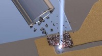
Så kallade "tvådimensionella" material har unika elektriska och fotoniska egenskaper, men deras ultratunna formfaktorer innebär praktiska utmaningar när de ingår i enheter. Penn Engineering-forskare har nu visat en metod för att göra "supergitter" med stor yta - skiktade strukturer som innehåller 2D-gitter av svavel och volfram - som kan uppnå lätt-materia-koppling. Kredit:University of Pennsylvania
Solpaneler, kameror, biosensorer och fiberoptik är teknologier som förlitar sig på fotodetektorer, eller sensorer som omvandlar ljus till elektricitet. Fotodetektorer blir mer effektiva och prisvärda, med deras komponenthalvledarchips som minskar i storlek. Denna miniatyrisering pressar dock mot gränser som sätts av nuvarande material och tillverkningsmetoder, vilket tvingar fram avvägningar mellan storlek och prestanda.
Det finns många begränsningar för den traditionella tillverkningsprocessen för halvledarchip. Chipsen skapas genom att halvledarfilmen växer över toppen av en wafer på ett sätt där filmens kristallina struktur är i linje med substratwaferns. Detta gör det svårt att överföra filmen till andra substratmaterial, vilket minskar dess användbarhet.
Dessutom görs den nuvarande metoden för att överföra och stapla dessa filmer genom mekanisk exfoliering, en process där en bit tejp drar av halvledarfilmen och sedan överför den till ett nytt substrat, lager för lager. Denna process resulterar i flera olikformiga lager staplade på varandra med varje lagers ofullkomlighet ackumulerad i helheten. Denna process påverkar kvaliteten på produkten samt begränsar reproducerbarheten och skalbarheten för dessa chips.
Slutligen, vissa material fungerar inte bra som extremt tunna lager. Kisel förblir allmänt förekommande som det valda materialet för halvledarchips, men ju tunnare det blir, desto sämre presterar det som fotonisk struktur, vilket gör det mindre än idealiskt i fotodetektorer. Andra material som presterar bättre än kisel eftersom extremt tunna lager fortfarande kräver en viss tjocklek för att interagera med ljus, vilket innebär utmaningen att identifiera optimala fotoniska material och deras kritiska tjocklek för att fungera i fotodetektorhalvledarchips.
Att tillverka enhetliga, extremt tunna, högkvalitativa fotoniska halvledarfilmer av annat material än kisel skulle göra halvledarchips mer effektiva, applicerbara och skalbara.
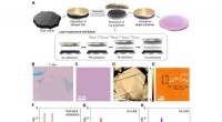
Penn Engineers Deep Jariwala, biträdande professor i elektro- och systemteknik, och Pawan Kumar och Jason Lynch, postdoktor och doktorand i hans labb, ledde en studie publicerad i Nature Nanotechnology som syftade till att göra just det. Eric Stach, professor i materialvetenskap och teknik, tillsammans med sin postdoc Surendra Anantharaman, doktoranden Huiqin Zhang och studentstudenten Francisco Barrera bidrog också till detta arbete. Samarbetsstudien inkluderade även forskare vid Penn State, AIXTRON, UCLA, Air Force Research Lab och Brookhaven National Lab, och finansierades i första hand av Army Research Lab. Deras artikel beskriver en ny metod för att tillverka atomärt tunna supergitter, eller halvledarfilmer, som är mycket ljusavgivande.
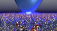
En atomtjocka material tar vanligtvis formen av ett gitter eller ett lager av geometriskt inriktade atomer som bildar ett mönster som är specifikt för varje material. Ett supergitter är uppbyggt av galler av olika material staplade på varandra. Supergitter har helt nya optiska, kemiska och fysikaliska egenskaper som gör dem anpassningsbara för specifika applikationer som fotooptik och andra sensorer.
Teamet på Penn Engineering gjorde ett supergitter, fem atomer tjockt, av volfram och svavel (WS2).
"Efter två års forskning med hjälp av simuleringar som informerade oss om hur supergittret skulle interagera med miljön, var vi redo att experimentellt bygga supergittret", säger Kumar. "Because traditional superlattices are grown on a desired substrate directly, they tend to be millions of atoms thick, and difficult to transfer to other material substrates. We collaborated with industry partners to ensure that our atomically thin superlattices were grown to be scalable and applicable to many different materials."
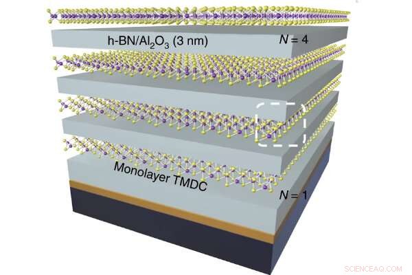
They grew monolayers of atoms, or lattices, on a two-inch wafer and then dissolved the substrate, which allows the lattice to be transferred to any desired material, in their case, sapphire. Additionally, their lattice was created with repeating units of atoms aligned in one direction to make the superlattice two-dimensional, compact and efficient.
"Our design is scalable as well," says Lynch. "We were able to create a superlattice with a surface area measured in centimeters with our method, which is a major improvement compared to the micron scale of silicon superlattices currently being produced. This scalability is possible due to uniform thickness in our superlattices, which makes the manufacturing process simple and repeatable. Scalability is important to be able to place our superlattices on the industry-standard, four-inch chips."
Their superlattice design is not only extremely thin, making it lightweight and cost effective, it can also emit light, not just detect it.
"We are using a new type of structure in our superlattices that involves exciton-polaritons, which are quasi-state particles made of half matter and half light," says Lynch. "Light is very hard to control, but we can control matter, and we found that by manipulating the shape of the superlattice, we could indirectly control light emitted from it. This means our superlattice can be a light source. This technology has the potential to significantly improve lidar systems in self-driving cars, facial recognition and computer vision."
Being able to both emit and detect light with the same material opens the door for more complicated applications.
"One current technology that I can see our superlattice being used for is in integrated photonic computer chips which are powered by light," says Lynch. "Light moves faster than electrons, so a chip powered by light will increase computing speed, making the process more efficient, but the challenge has been finding a light source that can power the chip. Our superlattice may be a solution there."
Applications for this new technology are diverse and will likely include high-tech robotics, rockets and lasers. Because of the wide range of applications for these superlattices, the scalability is very important.
"Our superlattices are made with a general, non-sophisticated process that does not require multiple steps in a clean room, allowing the process to be repeated easily," says Kumar. "Additionally, the design is applicable to many different types of materials, allowing for adaptability."
"In the tech world, there is a constant evolution of things moving toward the nanoscale," he says. "We will definitely be seeing a thinning down of microchips and the structures that make them, and our work in the two-dimensional material is part of this evolution."
"Of course, as we thin things down and make technology smaller and smaller, we start to interact with quantum mechanics and that's when we see interesting and unexpected phenomena occur," says Lynch. "I am very excited to be a part of a team bringing quantum mechanics into high-impact technology." + Utforska vidare