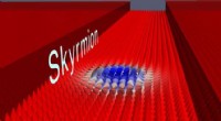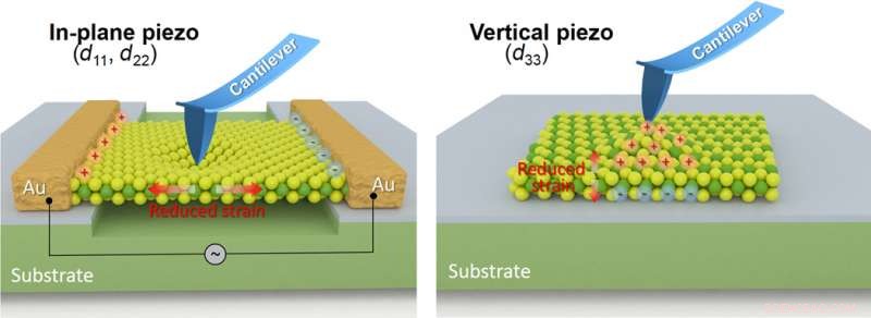
Fig. 1. Schematisk illustration av lokal karakterisering av piezoelektricitet i planet och vertikal piezoelektricitet. Piezoelektricitet i planet (piezo) ( d 11 , d 22 ) av ultratunna material är det plana elektromekaniska parbeteendet, där den applicerade spänningen och den producerade piezoelektriska potentialen är belägna i planet i det exponerade gitterplanet. Vertikal piezoelektricitet ( d 33 ) fokus på elektromekanisk interaktion inträffade i den vertikala axeln, som är vinkelrät mot materialytan. Högprecisionsdeformationsställdonet kan implementeras genom att använda exakt positionering av materialytan genom vertikal invers piezoelektricitet. Upphovsman:X. Wang, X. Han, H. Zhu, L. Sun, W. Fu, X. Wang, L. C. Hoong, H. Wang, Q. Zeng, W. Zhao, J. Wei, Z. Jin, Z. Shen, J. Liu, T. Zhang, Z. Liu, Subatomisk deformation driven av vertikal piezoelektricitet från CdS ultratunna filmer. Sci. Adv. 2, e1600209 (2016). Copyright © 2016 Författarna, vissa rättigheter reserverade; exklusiv licenstagare American Association for the Advancement of Science. Distribueras under en Creative Commons Attribution NonCommercial License 4.0 (CC BY-NC). DOI:10.1126/sciadv.1600209.
Piezoelektricitet ( aka den piezoelektriska effekten) förekommer i vissa material – kristaller (särskilt kvarts), lite keramik, ben, DNA, och ett antal proteiner – när tillämpningen av mekanisk stress eller vibration genererar elektrisk laddning eller växelströmsspänning, respektive. (Omvänt, piezoelektriska material kan vibrera när växelspänning appliceras på dem.) Den piezoelektriska effekten har ett stort antal användningsområden, inklusive ljudproduktion och detektering, generering av höga spänningar och elektroniska frekvenser, atomupplösningsavbildningstekniker (t.ex. scanning tunneling och atomic force mikroskopi), och ställdon för mycket exakt positionering av objekt i nanoskala – det sista är avgörande för grundläggande forskning och industriella tillämpningar. Med det sagt, Positionering i subatomär skala innebär fortfarande ett antal utmaningar. Nyligen, dock, forskare vid Nanyang Technological University, Singapore, kinesiska vetenskapsakademin, Suzhou, och Duke University, Durham demonstrerade vertikal piezoelektricitet i atomär skala (tre till fem rymdgitter) med hjälp av ultratunna kadmiumsulfid (CdS) filmer. Forskarna bestämde en vertikal piezoelektrisk koefficient ( d 33 ) tre gånger så mycket som bulk CdS som använder på plats scanning Kelvin kraftmikroskopi och enkel och dubbel ac resonansspårning piezoelektrisk kraftmikroskopi, får dem att dra slutsatsen att deras resultat har ett antal kritiska roller i utformningen av nästa generations sensorer och mikroelektromekaniska enheter.
Prof. Zheng Liu diskuterade uppsatsen att han, Dr Ting Zhang och deras kollegor publicerade i Vetenskapens framsteg , beskriver en serie utmaningar som de ställdes inför och började med att använda kemisk ångavsättning för att syntetisera 2~3 nm kadmiumsulfid (CdS) tunna filmer. "Den vertikala piezoelektriciteten, eller d 33 , är nyckelparametern i piezoelektriska material för tillverkning av ställdon som används för att positionera objekt med extrem noggrannhet – ner till atomär skala i ett brett utbud av banbrytande utrustning som atomkraftsmikroskopi och skanningstunnelmikroskopi, " berättar Liu Phys.org . "Dessutom, Högpresterande ultratunna piezoelektriska material är avgörande för att konstruera ultrahög upplösning och flexibla elektromekaniskt kopplade enheter."
Före denna studie, Liu påpekar, endast några få studier rapporterade syntesen av atomära tunna piezoelektriska material med en våtkemisk metod, exempel på dessa inkluderar CdS och kadmiumselenid (CdSe) nanotrombocyter. "Det är en betydande utmaning att producera högkvalitativa och atomtunna piezoelektriska material, " tillägger han. "I denna forskning, den största utmaningen vid syntetisering av ultratunna piezoelektriska CdS -filmer via kemisk ångavsättning "(eller CVD)" ligger i valet av prekursorer och hur man optimerar reaktionsparametrarna, såsom växande temperatur och tid."
Forskarna ställdes sedan inför demonstration d 33 vertikal piezoelektricitet i atomär skala med hjälp av ultratunna kadmiumsulfid tunna filmer. "När materialets tjocklek når nanoskala, "Liu förklarar, "det är mycket svårt att verifiera den piezoelektriska effekten och bestämma dess värden på grund av kopplingseffekten från substratet - och ytgeometrier kan också påverka mätningarna vid atomgränser." Till exempel, han illustrerar, provets ytråhet når tiotals pikometer, vilket är samma skala med den vertikala elektromekaniska responsen för material.
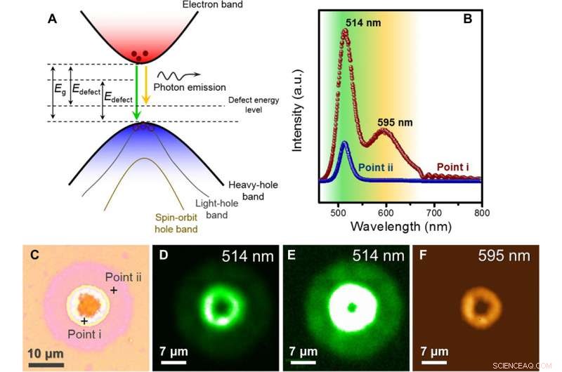
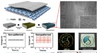
Fig. 3. Spektroskopisk karakterisering av CdS-tunnfilm. (A) Energi ( E ) bandstruktur i närheten av Γ-punkten i Brillouin-zonen, som visar fotonemissionsprocessen. (B och C) PL-spektrum av CdS-tunnfilm från punkterna i och ii markerade i (C) med plustecken, visar stark bandkantemission (506 nm) av CdS ultratunn film och defektrelaterad emission (595 nm). (C) Optisk bild av tunn CdS-film med en rundad mikropartikel i mitten. a.u., godtyckliga enheter. (D och E) PL -kartläggning vid en emission av 514 nm med en annan skala bar, uppvisar hög enhetlighet och homogenitet för CdS-tunna filmer på utsidan. (F) PL-kartläggning vid 595 nm-utsläpp, vilket indikerar att den defektrelaterade emissionen endast sker vid den tjockare CdS-mikropartikeln. Upphovsman:X. Wang, X. Han, H. Zhu, L. Sun, W. Fu, X. Wang, L. C. Hoong, H. Wang, Q. Zeng, W. Zhao, J. Wei, Z. Jin, Z. Shen, J. Liu, T. Zhang, Z. Liu, Subatomisk deformation driven av vertikal piezoelektricitet från CdS ultratunna filmer. Sci. Adv. 2, e1600209 (2016). Copyright © 2016 Författarna, vissa rättigheter reserverade; exklusiv licenstagare American Association for the Advancement of Science. Distribueras under en Creative Commons Attribution NonCommercial License 4.0 (CC BY-NC). DOI:10.1126/sciadv.1600209.
Till sist – och påminner om utmaningen att demonstrera d 33 vertikal piezoelektricitet i atomär skala med hjälp av tunna CdS-filmer – forskarna var tvungna att bestämma den vertikala piezoelektriska koefficienten för CdS-filmen med på plats scanning Kelvin kraftmikroskopi (SKFM) och enkel och dubbel AC resonansspårning piezoelektrisk kraftmikroskopi (DART-PFM). "Kvaliteten på ultratunn piezoelektrisk CdS är nyckeln till att få en pålitlig vertikal piezoelektrisk koefficient." Liu noterar. "Vissa karaktäriseringsverktyg som Raman och fotoluminescensspektroskopier kan hjälpa oss att identifiera CdS-provet och bekräfta dess höga kvalitet. Dessutom, på grund av de geometriska vibrationerna i CdS-proverna, the atomic force microscopy characterization should be carefully carried out in order to make sure our conclusions are solid." This required the researchers to examine many SKFM and DART-PFM samples using to reach a solid conclusion about vertical piezoelectric behavior in CdS ultrathin films.
Liu comments that addressing these challenges required innovative techniques. "För första gången, we successfully synthesized high-quality atomic thin CdS films using CVD, and we demonstrated vertical piezoelectricity of these films at the atomic scale of 3~5 space lattices" (a space, or crystal, lattice being a periodically repeating two- or three-dimensional array of points or particles) "and observed the vertical piezoelectric domains. More importantly, " Liu continues, "our work shows an enhanced vertical piezoelectricity in CdS ultrathin films at a level three times larger than the CdS bulk counterpart, as well as higher than most of traditional piezoelectric materials." These results imply non-trivial piezoelectric behavior at atomic limits for a certain class of materials – which has not yet been well explored – and inspires the search for two-dimensional free-standing layered piezoelectric materials that are only one atom thick.
Liu points out that their findings shed light on the design of next-generation sensors, actuators and microelectromechanical devices, in that piezoelectric materials are the most important component for such devices. Specifikt, he says that their findings provide the opportunity for next-generation sensors and microelectromechanical devices in three ways:
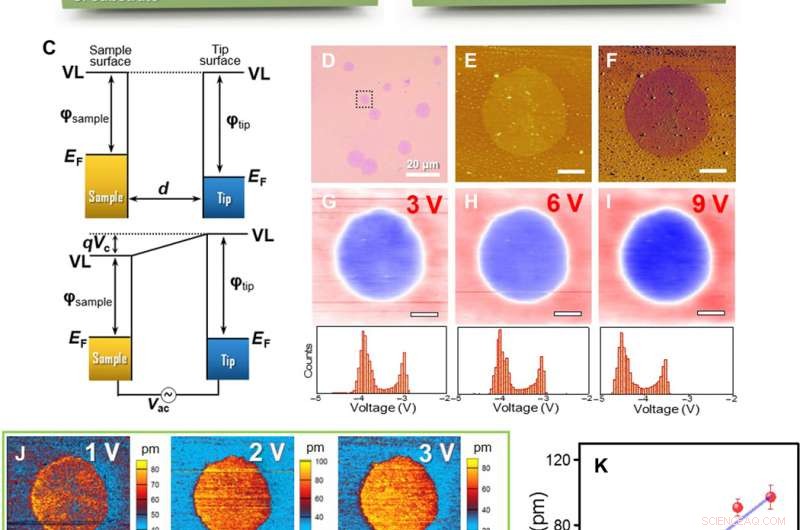
Fig. 4. Noncontact SKFM and standard contact PFM investigation for CdS thin film. (A and B) Schematic illustration of SKFM (A) and PFM (B) measurements. (C) Band diagram of tip and sample when they are electrically separated (top graph) and electrically contacted (bottom graph). d , distance; VL, vacuum levels; q , electronic charge; V c , contact potential difference. (D) Optical image of CdS thin films. (E and F) Topography (E) and phase (F) images observed by SKFM mode for the single CdS thin film marked in (D). (G to I) Corresponding potential mappings with tip voltages of 3, 6, and 9 V, respektive. Insets show histograms of the surface potential distributions. The CdS ultrathin film has a higher positive voltage (~0.9 V) than the substrate, demonstrating that a large amount of charges are accumulated at a CdS thin film after contact PFM scanning. (J) Amplitude images observed by contact PFM technology with tip voltages from 1 to 6 V, showing remarkable inverse piezoelectricity. (K) Average amplitude variations versus applied voltages calculated from (J). Error bars indicate 1 SD. Scale bars, 2 μm (E to J). The linearly fitted line shows that the measured piezoelectric coefficient d eff is ~16.4 pm·V −1 , whereas the vertical piezoelectric coefficient d 33 is ~32.8 pm·V −1 . Credit:X. Wang, X. He, H. Zhu, L. Sun, W. Fu, X. Wang, L. C. Hoong, H. Wang, Q. Zeng, W. Zhao, J. Wei, Z. Jin, Z. Shen, J. Liu, T. Zhang, Z. Liu, Subatomic deformation driven by vertical piezoelectricity from CdS ultrathin films. Sci. Adv. 2, e1600209 (2016). Copyright © 2016 The Authors, some rights reserved; exclusive licensee American Association for the Advancement of Science. Distributed under a Creative Commons Attribution NonCommercial License 4.0 (CC BY-NC). DOI:10.1126/sciadv.1600209.
Liu illustrates these points by listing potential examples of such devices – for example, atomically thin piezoelectric devices – and their applications. "Till exempel, using CdS ultrathin films, the most accurate probe or stage ever fabricated may be achievable, allowing researchers and engineers to manipulate atoms or position tips in atomic force, scanning electron and transmission electron microscopy. Med andra ord, CdS ultrathin films will extend our capability to see and manipulate our world in an extreme way." Of more importance, han lägger till, such ultrathin piezoelectric devices can be integrated into equipment like autocollimators and Michelson interferometers used in, for example, cold atom studies, the verification of the gravitational inverse square law at short range, and even the detection of gravitational waves.
The study also reports the på plats measurement of the ultrathin CdS film vertical piezoelectric coefficient d 33 , determining the film coefficient to be approximately three times larger than that of bulk CdS. "This value is pretty big for atomically thin materials, " Liu explains. "It means that we can get a large voltage change when small pressure or deformation is applied. This makes the material a great candidate constructing sensitive and ultrathin mechanical sensors."
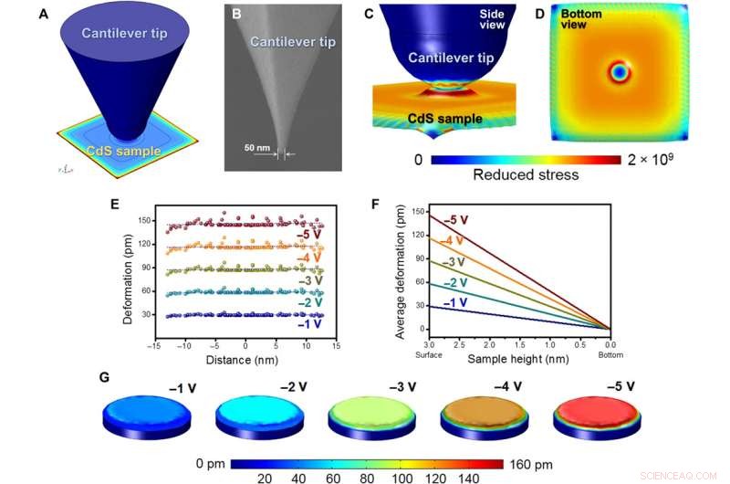
Fig. 6. Simulation of vertical piezoelectricity and subatomic deformation actuator. (A) Three-dimensional image of potential drop on CdS film. (B) Scanning electron microscopy image of a conductive tip for PFM characterization. (C and D) Bottom and side views of stress distribution on CdS film. (E to G) Simulation for subatomic deformation actuator. Different potentials were applied to surface deformation curves (E), mappings (G), and vertical deformation (F) of CdS thin films. Credit:X. Wang, X. He, H. Zhu, L. Sun, W. Fu, X. Wang, L. C. Hoong, H. Wang, Q. Zeng, W. Zhao, J. Wei, Z. Jin, Z. Shen, J. Liu, T. Zhang, Z. Liu, Subatomic deformation driven by vertical piezoelectricity from CdS ultrathin films. Sci. Adv. 2, e1600209 (2016). Copyright © 2016 The Authors, some rights reserved; exclusive licensee American Association for the Advancement of Science. Distributed under a Creative Commons Attribution NonCommercial License 4.0 (CC BY-NC). DOI:10.1126/sciadv.1600209.
The researchers concluded that contact piezoresponse force microscopy (PFM) – which uses a conductive tip to apply a highly localized electric field that allows imaging and manipulation of piezoelectric ferroelectric materials – could significantly change the surface potential of a CdS ultrathin film by applying stress to its surface. "Vanligtvis, applying mechanical stress to a piezoelectric material will generate electric charge that accumulates at the surface of the material, which is how we identify the piezoelectric materials, " berättar Liu Phys.org . "We therefore believe that this results from piezoelectric polarizations giving rise to a large piezoelectric potential, in turn leading to a remarkable spatial separation of electrons and holes." In this case, electrons generated by the piezoelectric effect will be trapped into the silicon dioxide (SiO 2) dielectric layers, while the holes will be trapped inside the crystal boundary of the CdS films.
The scientists state that their work may pave a way to the synthesis of ultrathin lattice scale nanomaterials using CVD method, which is a low-cost method for producing high quality samples. Dessutom, Liu notes, the materials provided by their study will enable the high-integrated and multi-functional devices by simply coating or transferring the film to the device. "For actuator applications, our work will promote next generation actuators with extreme resolution for their potential use in characterization tools such as ultra-high resolution microscopy; for atom manipulation and fabrication; or potentially for the detection of ultra-low deformation in, for example, cold atom studies, verification of the gravitational inverse square law at short range, and even the detection of gravitational waves."
Går vidare, Liu says, the scientists will determine the relationship between the vertical piezoelectric coefficient d 33 and the thickness of CdS at atomic scales. "Well also synthesize other piezoelectric, ferroelectric and layered piezoelectric/ferroelectric ultrathin materials, and explore their electromechanical properties." Based on this material and micro/nano-manufacture technology, the researchers hope to design and fabricate next-generation actuators for accurate positioning of minute objects, such as nanoparticles at subatomic scales, using their novel materials.
Dessutom, the large vertical piezoelectric coefficient d 33 makes this material promising to construction of ultrathin and sensitive pressure sensors for detecting miniscule forces. If the low detection limit of sensor reaches to nanoscale levels, the device could monitor single biological cell migration.
"Our study will inspire material scientists to hunt for other non-trivial ultrathin or layered piezoelectric or ferroelectric materials, " berättar Liu Phys.org . "Engineers can employ our CdS ultrathin films to design and fabricate novel microelectromechanical systems, " or MEMS, "and nanoelectromechanical systems, " or NEMS, "with high-integration and multi-functionalities, and may benefit when developing cutting-edge scientific instruments. Vidare, " he concludes, "novel and flexible consumer electronic devices can be developed based on our study."
© 2016 Phys.org