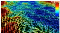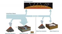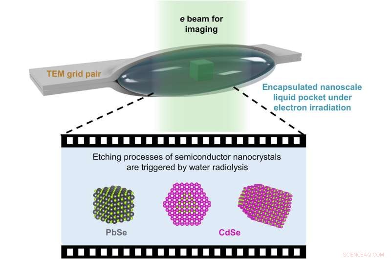
Illustration av LCTEM-experimenten. Tvärsnittsvyn visar att ett tunt vattenhaltigt skikt innehållande halvledarnanokristaller är inklämt mellan två ultratunna kolfilmer av ett par TEM-galler. Elektronstrålen som passerar genom vattnet och kolskikten orsakar vattenradiolysreaktioner, som sedan utlöser etsbanorna för att avbildas med LCTEM. Kredit:Science Advances (2022). DOI:10.1126/sciadv.abq1700
Halvledarnanokristaller av olika storlekar och former kan styra materialens optiska och elektriska egenskaper. Liquid cell transmission electron microscopy (LCTEM) är en framväxande metod för att observera kemiska transformationer i nanoskala och informera om den exakta syntesen av nanostrukturer med förväntade strukturella egenskaper. Forskare undersöker reaktionerna hos halvledarnanokristaller med metoden att studera den mycket reaktiva miljö som produceras via flytande radiolys under processen.
I en ny rapport som nu publicerats i Science Advances , Cheng Yan och ett forskarlag i kemi och materialvetenskap vid University of California Berkeley, och Leibniz Institute of Surface Engineering, Tyskland, utnyttjade radiolysprocessen för att ersätta den enstaka partikeletsningsbanan för prototypiska halvledarnanomaterial. Bly selenid nanorör som användes under arbetet representerade en isotrop struktur för att behålla den kubiska formen för etsning genom en lager-för-lager-mekanism. De anisotropa pilformade nanoroderna av kadmiumselenid bibehöll polära aspekter med kadmium- eller selenatomer. Banorna för transmissionsvätskecellelektronmikroskopi avslöjade hur reaktiviteten hos specifika aspekter i flytande miljöer styrde formtransformationerna i nanoskala av halvledare.
Optimering av flytande celltransmissionselektronmikroskopi (LCTEM)
Halvledarnanokristaller innehåller brett avstämbara optiska och elektriska egenskaper som beror på deras storlek och form för en mängd olika applikationer. Materialforskare har karakteriserat reaktiviteten hos specifika bulkkristallfacetter mot tillväxt och etsningsreaktioner för att utveckla de mest godtyckliga mönstren i top-down bulkhalvledarbearbetning. De många aspekterna av nanokristaller och deras reaktionsmekanism gör dem intressanta för direkt undersökning. Termodynamiken hos kolloidala nanokristaller kan påverka de organiskt-oorganiska gränssnitten som definierar dem. Flytande celltransmissionselektronmikroskopi erbjuder den nödvändiga rymd-tidsupplösningen för att observera nanoskala dynamik, såsom självmonteringsprocessen. Teamet placerade därför en vattenhaltig ficka innehållande nanokristaller mellan de ultratunna kolskikten i två transmissionselektronmikroskopinät och använde tris (hydroximetyl) aminometanhydroklorid (tris·HCl), en organisk molekyl för att reglera etsningen av känsliga halvledarnanokristaller.
Befintlig forskning om LCTEM och nanokristaller är begränsad till ädelmetaller på grund av deras oförmåga att reglera den kemiska miljön under radiolys, vilket gör att reaktiva material bryts ned. Ny forskning tyder på en möjlighet att designa nya miljöer för LCTEM, för att observera enpartikeletsningsbanor för reaktiva nanokristaller. Under experimenten reglerade tris·HCl-tillsatsen den elektrokemiska potentialen för etsningsprocessen, och teamet använde kinetisk modellering för att uppskatta koncentrationen och den elektrokemiska potentialen för aminradikalarterna i den flytande cellen.
Proof-of-concept
As proof of concept, the scientists obtained representative transmission electron microscopy images of a lead selenide nanocube in vacuum and gathered a time-series of images during layer-by-layer etching of lead selenide nanocrystals. The outcome of LCTEM imaging showed the formation of a substance with higher image contrast around the lead selenide nanocrystals as a product of etching reactions, it appears that during the etching process, selenium oxidized and dispersed into the liquid to facilitate the formation of lead chloride, with chloride ions in the lead pocket. When compared to the cubic lattice of lead selenide, wurzite cadmium selenide featured an anisotropic lattice with alternating layers of cadmium and selenium atoms. During the growth of wurzite cadmium selenide nanocrystals, the surfactant ligands favorably bound to the cadmium regions to facilitate the fast growth of selenium regions.
Yan et al. presented the structure of cadmium selenide nanorods resolved via high-angle annular dark field scanning transmission electron microscopy in vacuum. The scientists generated the images by collecting electrons scattered to high angles by atoms in the material to develop mass-thickness image contrast, where cadmium was brighter than selenium. The team similarly performed in situ etching experiments on arrow-shaped cadmium selenide nanorods.
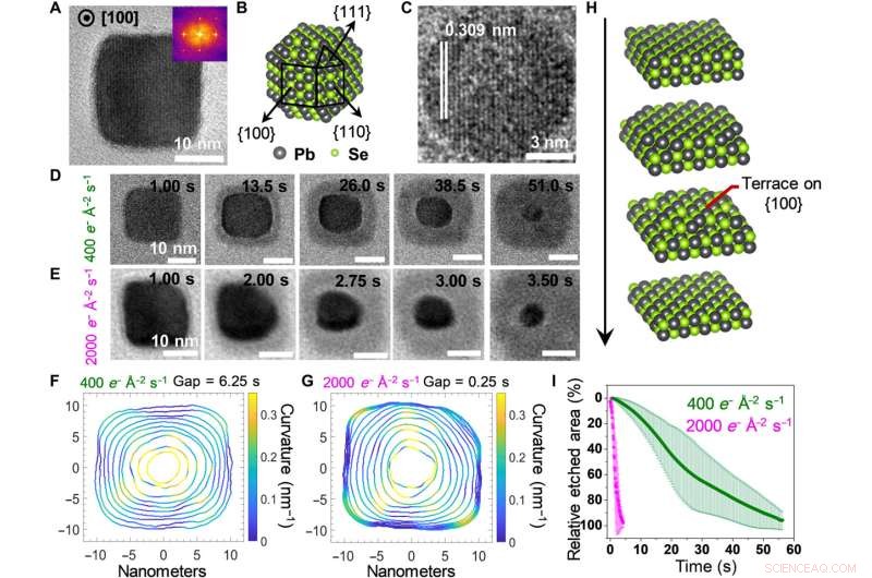
Structural characterization and etching trajectories of PbSe nanocubes. (A) Representative static TEM image of a PbSe nanocube oriented along the [100] zone axis. (B) Atomistic model of a truncated PbSe nanocube exposing different facets. (C) The LCTEM image captured near the end of an etching trajectory, exhibiting the characteristic d-spacing of {200} lattice planes of PbSe. (D and E) Time-lapse LCTEM images recorded at the electron fluence rates of 400 e− Å−2 s−1 (D) and 2000 e− Å−2 s−1 (E), respectively. (F and G) Outlines of the nanocrystals plotted with equal time gaps for illustrating the evolving shapes and local curvatures of PbSe nanocrystals recorded at 400 e− Å−2 s−1 (F) and 2000 e− Å−2 s−1 (G), respectively. (H) Scheme of the layer-by-layer etching mechanism, which proceeds via terrace intermediates. (I) The time-dependent plots of the relative etched area normalized to the projected area of the PbSe nanocube at the starting frame. Kredit:Science Advances (2022). DOI:10.1126/sciadv.abq1700
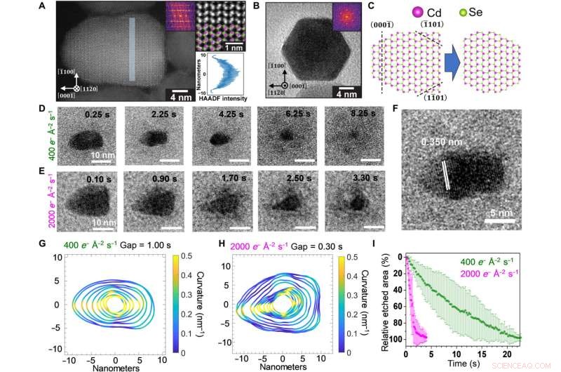
Structural characterization and etching trajectories of CdSe nanorods. (A) AC-HAADF-STEM image of a wurtzite CdSe nanorod projected along the [110] zone axis (left). The enlarged inset (top right) verifies the polarity of the nanorod:The tip of the rod is terminated by Se (green), while the bottom is terminated by Cd (pink). The line profile of HAADF-STEM intensity in the shaded segment (left) projected along the [00] axis is included in the bottom right. (B) TEM image of a nanorod oriented along the c axis showing a hexagonal projection. (C) Lattice models of a CdSe nanorod projected along the [110] axis (left) and the truncated structure (right) formed by selectively etching the Se-terminated facets. (D and E) Time-lapse LCTEM images recorded at electron fluence rates of 400 e− Å−2 s−1 (D) and 2000 e− Å−2 s−1 (E), respectively. (F) The LCTEM image exhibiting the characteristic d-spacing of {0002} lattice planes. (G and H) Outlines of the nanocrystals plotted with equal time gaps for illustrating the evolving shapes and local curvatures of CdSe nanorods at 400 e− Å−2 s−1 (G) and 2000 e− Å−2 s−1 (H), respectively. (I) Time-dependent plots of the relative etched area normalized to the projected area of the CdSe nanorod at the starting frame. Kredit:Science Advances (2022). DOI:10.1126/sciadv.abq1700
The etching trajectory of a wurtzite CdSe nanocrystal viewed along the [000] axis. (A) Time-lapse LCTEM images recorded at 400 e− Å−2 s−1. (B) Atomistic model of the CdSe nanocrystal with the (000) facet pointing up. (C) Time-dependent plot of the average electron fluence rates detected in different color-coded segments (inset) of the LCTEM images. Gray color corresponds to the background region surrounding the nanocrystal. (D) 3D illustration of the etching process showing that the selective etching of the Se-terminated (000) facet causes the tip to transform into a concave pit in the nanocrystal. Kredit:Science Advances (2022). DOI:10.1126/sciadv.abq1700
In this way, Cheng Yan and colleagues used liquid cell electron microscopy (LCTEM) to show the possibility of directly examining the facet-dependent reactivity of colloidal nanocrystals at the nanoscale. The method offered real-time, continuous structural trajectories, in contrast to classical methods. Existing research had already highlighted the effect of the inclusion or removal of ligands on the self-assembly and etching of nanocrystals in LCTEM experiments.
The team showed how sensitive nanomaterials such as lead selenide can be studied using LCTEM and highlighted the inclusion of organic additives such as tris·HCl to regulate the radiolytic redox environment in liquid cell electron microscopy. Future studies can enable the potential to gain real-time information about the transformation of an array of functional nanostructures with increasing complexity using core/shell nanocrystals, as well as those assembled via inorganic-organic interfaces. + Utforska vidare
© 2022 Science X Network